Market Now
[From the Scene] Samsung spurring innovation from Silicon Valley
 |
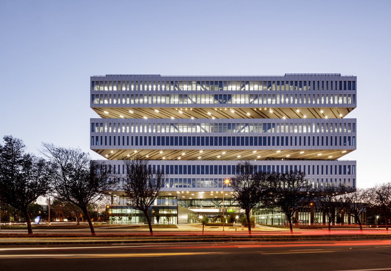
The Samsung Electronics Device Solutions America headquarters in San Jose, California (Samsung Electronics) |
 |
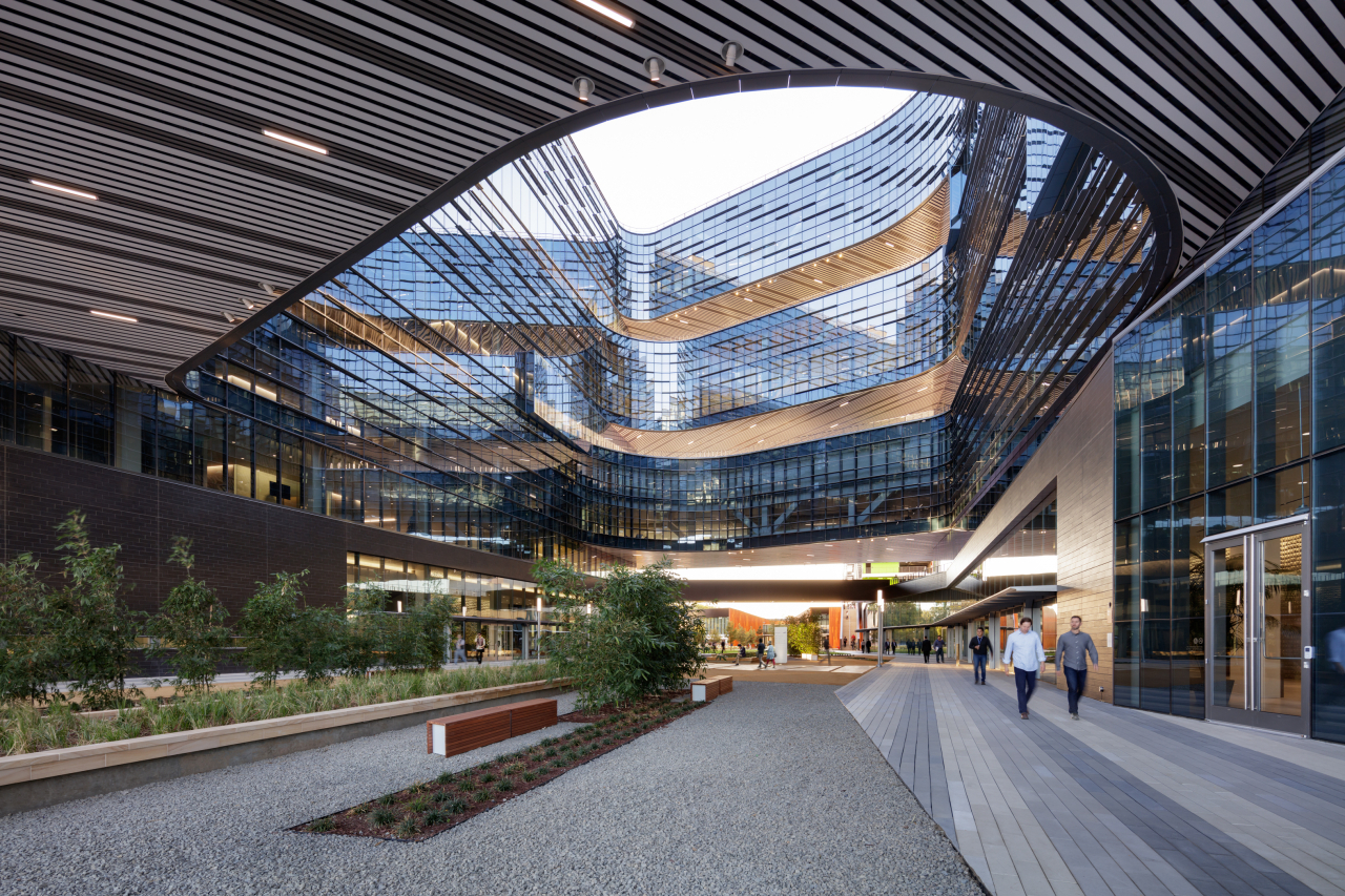
The Samsung Electronics Device Solutions America headquarters in San Jose, California (Samsung Electronics) |
SAN JOSE, California -- At the heart of Silicon Valley, home to world's largest tech giants, stands a landmark 10-story building in the shape of a three-layer stack of NAND flash memory chips.
The symbolic building is the headquarters of Samsung Electronics Device Solutions America, which oversees the production of semiconductors in the United States -- a market that takes up more than half of the global chip demand.
Opening the US headquarters to Korean media on Saturday, Sue Kim, the head of DS Marketing, explained Samsung's strong presence in the US.
“Samsung is much more well appreciated in the US than what people may think in Korea. Koreans here can work with dignity in Silicon Valley, where excellent talent of different cultures reside. This is because Samsung’s brand value, which is founded on its advanced technology, plays a big role,” Kim said.
Samsung Electronics established the DS America office in 1983, when it started developing the 64Kb DRAM. The office’s symbolic outward structure, representing three memory chips, was newly built in 2015.
When The Korea Herald visited the headquarters, an employee was seen jogging on a treadmill, looking out a glass walled window of a gym on the fifth floor. The building, wrapped in glass, has a full gym, basketball courts and other sports facilities.
The gym is not the only facility open on weekends for employees. The marketing chief also noted that the office's in-house cafeteria is the "only office in Silicon Valley" offering Korean cuisine year-round. Other cuisines, including American, Japanese, Chinese and Mexican are offered for executives and employees of different cultural backgrounds, Kim added.
At the headquarters, some 1,200 employees work on semiconductor research and development, as well as sales and marketing. It also has research divisions for the company's memory chips, system Large Scale Integration and foundry businesses that work closely with the Seoul headquarters, according to officials.
"DS America aims to strengthen the competitiveness of Samsung’s semiconductor business in the US, and plays a role of consolidating R&D, sales, marketing and customer support capabilities,” said Han Jin-man, the vice president of DS America.
 |
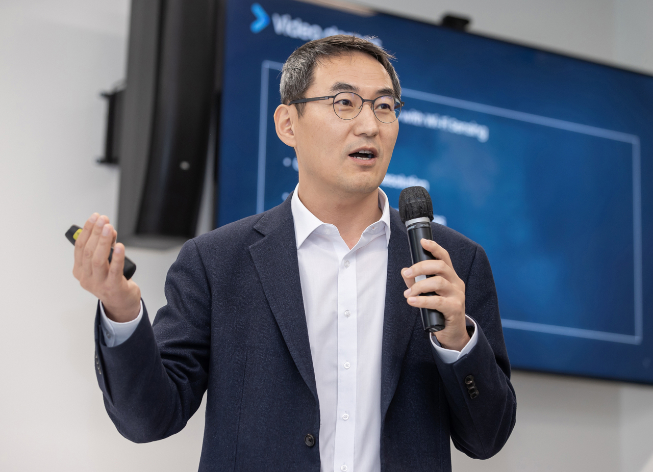
Samsung Research American Vice President Roh Won-il speaks to reporters at the SRA headquarters in Mountain View, California, Saturday. (Samsung Electronics) |
SRA, where the most advanced tech is developed
Just 10 minutes away by car from the DSA headquarters is Samsung Research America, one of the 15 research institutes the Korean tech giant operates in 14 countries.
The SRA oversees the conglomerate’s most advanced technologies for the Device eXperience division, which is the company’s home appliances and mobile device businesses.
“The keywords I choose to describe our center is ‘foundation of innovative excellence," SRA President Roh Won-il told reporters.
"This area is expensive -- both the land and talent. Still, there are a lot of excellent technicians. With the human resources, my goal is to raise our technical excellence to the top notch and lead innovation by acquiring core technologies and patents."
About 650 researchers work at the SRA, working on next-generation technologies for telecommunications and artificial intelligence, as well as robots and digital health, multimedia, camera and software platforms, the company said.
One of the focus areas for the SRA is telecommunications. Its researchers first discovered the cutting-edge beamforming technology, which can enable application of the mmWave 5G. In 2021, researchers succeeded in demonstrating the 6G Terahertz wireless communication prototype.
The SRA also operates seven Artificial Intelligence Centers in five countries including South Korea, the US, the UK, Canada and Russia.
By Jo He-rim
Korea Herald correspondent (herim@heraldcorp.com)


