Market Now
Samsung starts mass production of world’s first 3-nm chips
 |
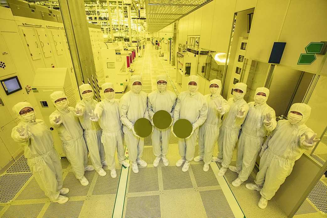
Samsung Electronics executives and researchers pose with semiconductor wafers, produced by 3-nm technology, at the company’s chip-making complex in Hwaseong, Gyeonggi Province, on Thursday. (Samsung Electronics) |
Samsung Electronics said Thursday it has started producing chips using its latest 3-nanometer manufacturing technology -- an industry first globally.
The 3-nm technology boasts greater transistor density than the current 5-nm technology, which means higher speed and lower power consumption of advanced chips for artificial intelligence, big data and autonomous cars.
Samsung, the world’s largest memory chipmaker, hopes to wield the new technology as a weapon in taking on Taiwan’s TSMC, the dominant leader in the lucrative foundry market.
According to market tracker TrendForce, TSMC took up 52.1 percent of the global foundry market in the fourth quarter last year, while Samsung remained a distant No. 2 with an 18.3 percent share.
Samsung’s 3-nm technology is also the first to use the most advanced transistor architecture, called gate-all-around field-effect transistor technology (GAAFET) which has increased the overall efficiency of the current fin field-effect transistor technology (FinFET).
Samsung trademarked its own GAAFET technology as “Multi-Bridge-Channel FET.”
As the result of overall technological upgrades, Samsung said its first-generation 3-nm process has reduced power consumption by 45 percent and improved performance by 23 percent, compared to the current 5-nm process using FinFET.
For the second generation, power consumption is expected to be cut in half, with performance being boosted by 30 percent, the firm added.
“Samsung has grown rapidly as we continue to adopt the foundry industry’s first technologies like High-K Metal Gate, FinFET and EUV,” said Choi Si-young, president and head of foundry business at Samsung. EUV refers to extreme ultraviolet lithography. “We will continue active innovation in competitive technology development and build systems that help expedite our achievement of technological maturity.”
GAAFET is considered essential for next-generation foundry microfabrication, which is smaller than 3 nm, but chipmakers are struggling to elevate the yield rate of the highly sophisticated manufacturing technology.
TSMC also plans to start mass-producing the 3-nm chips later this year, but would continue to use the FinFET largely for stability.
“Samsung is taking risks by adopting the 3-nm process earlier than its rivals amid concerns over the low yield rate in the earlier stage,” said an industry source who wished to be unnamed.
“It may be difficult for Samsung to take shares from TSMC immediately, but it could seek an upper hand at least in the nascent 3-nm process.”
During a first-quarter conference call in April, Samsung executives dismissed concerns over the initial yield rate, saying they have reduced the ramp-up period by enhancing inspection throughout the development process.
They also showed confidence in elevating profitability, citing robust market demand and strong client partnerships.
The latest breakthrough comes as Samsung Electronics Vice Chairman Lee Jae-yong, the de facto leader of the nation’s largest company, has renewed his commitment to “super-gap” technologies.
“First is technology, second is technology and third is also technology,” the Samsung chief said upon his return from a business trip to Europe earlier this month.
One of the key destinations of his two-week trip was the Netherlands, home to ASML, the sole producer of EUV systems that are crucial to making advanced chips.
During the visit, he held meetings with Dutch Prime Minister Mark Rutte and ASML CEO Peter Wennink to ask support for Samsung to secure more ASML machines that are currently in tight supply due to chip shortages.
When US President Joe Biden visited Seoul in May, he and President Yoon Suk-yeol signed a semiconductor wafer, not a visitors’ book, during their visit to Samsung’s chip manufacturing complex in Pyeongtaek, Gyeonggi Province.
It was the first time that the wafer, produced by Samsung’s 3-nm technology, was unveiled to the public.
By Lee Ji-yoon (jylee@heraldcorp.com)


![[Contribution] Preparing for future with strategic public procurement](http://res.heraldm.com/phpwas/restmb_idxmake.php?idx=151&simg=/content/image/2024/11/29/20241129050037_0.jpg)
