Market Now
Samsung chief visits ASML HQ as race for high-end chip intensifies
 |
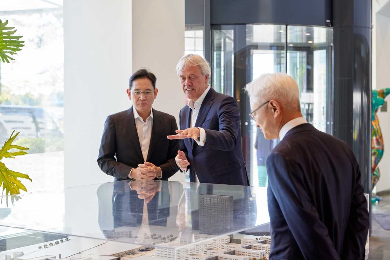
ASML CEO Peter Wennink (right) greets Samsung Electronics Vice Chairman Lee Jae-yong (left) at the Dutch chip equipment giant’s headquarters in Eindhoven, the Netherlands, on Tuesday. (Samsung Electronics) |
Samsung Electronics top executives on Tuesday held talks with representatives of chip photolithography equipment maker ASML, including its Chief Executive Officer Peter Wennink, the South Korean tech giant said Wednesday.
Representatives of Samsung, including Lee Jae-yong, vice chairman and de facto leader; and Kyung Kye-hyun, co-chief executive officer in charge of Samsung’s semiconductor business, visited the headquarters of ASML in Eindhoven, the Netherlands.
Samsung said in a statement that the meeting was held to discuss ways to handle supply issues of ASML’s extreme ultraviolet photolithography solutions, which are considered key to the world‘s most-advanced semiconductor chip manufacturing process. ASML is the sole provider of EUV solutions in the world.
Samsung, a minority shareholder of ASML, did not elaborate further on their discussions.
Tuesday’s meeting came 20 months after Lee and Wennink last met at the ASML headquarters in October 2020.
This reflects the world‘s race for high-end semiconductor chips amid chip supply shortage. It also highlights the need to secure the rare equipment, using extremely short wavelengths to print tiny circuit patterns onto wafer-thin materials.
Samsung first adopted the EUV technology in its 7-nanometer process in its contract-based chip manufacturing in 2017. The company also began mass producing 10-nanometer DRAMs in 2020 through EUV process. Its crosstown rival SK hynix moved in tandem, introducing EUV process to its DRAM manufacturing in 2021.
While ASML’s EUV machines have primarily been sold to Korea and Taiwan, home to the world‘s largest foundry TSMC, more chip manufacturers are looking to secure the machines. Intel earlier this year unveiled plans to adopt a 2-nanometer process using ASML’s EUV equipment starting in 2024.
Samsung made a strategic investment in ASML with chip giants Intel and TSMC in 2012. Fewer than 50 EUVs have been manufactured each year.
In the meantime, Lee also met with Dutch Prime Minister Mark Rutte earlier in the day to discuss a chip partnership between the two countries.
Their meeting came six years since their last in Korea in September 2016. At the time, Lee offered Rutte a personal tour around Samsung’s corporate exhibition center in Seoul and introduced the company’s business plans and latest technologies.
The Netherlands boasts an advanced industrial ecosystem for chipmaking ranging from research and development to equipment and finished products. South Korea, the world’s largest memory chip exporter, has continued bolstering ties with the country.
In his first phone call with the Dutch PM, then-President-elect Yoon Suk-yeol stressed his will to help elevate the bilateral partnership between the two countries, calling chips “rice for the future.”
With his latest trip to Europe, Lee aims to inspect Samsung’s business operations there and shore up his personal network, with his every move and meeting being scrutinized for potential links to new deals. Lee flew to Belgium to visit Interuniversity Microelectronics Center Wednesday and is scheduled to return home Saturday.
By Son Ji-hyoung (consnow@heraldcorp.com)


![[Exclusive] Hyundai Mobis eyes closer ties with BYD](http://res.heraldm.com/phpwas/restmb_idxmake.php?idx=151&simg=/content/image/2024/11/25/20241125050044_0.jpg)


